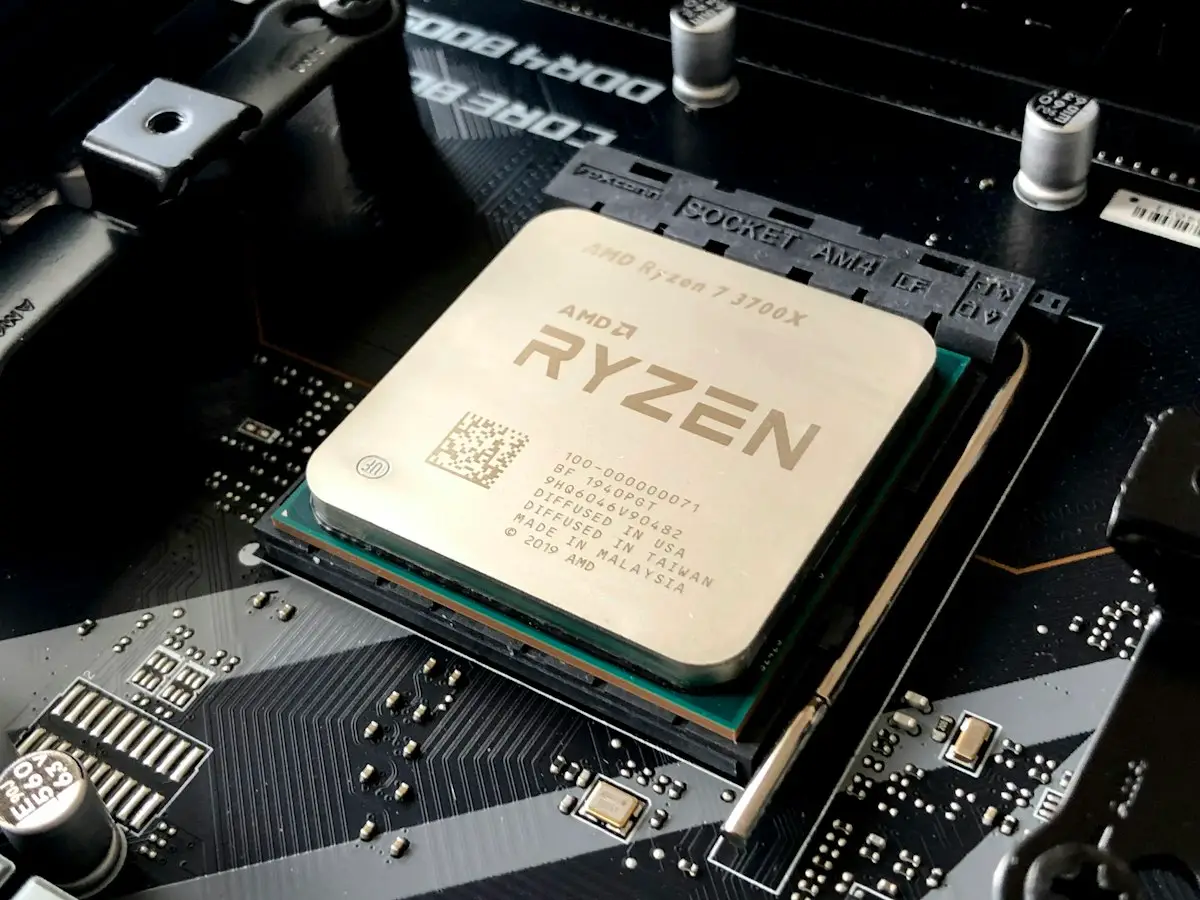
TSMC has initiated risk production on its 2nm N2 process node at Fab 20 in Hsinchu, marking the foundry’s commercial transition from FinFET transistors to Gate-All-Around (GAA) nanosheet structures. The milestone sets the silicon schedule for next-generation consumer flagships and hyperscale AI accelerators expected in late 2026 and early 2027.
Transistor Scaling Reaches the GAA Threshold
The N2 architecture replaces traditional 3D FinFET fins with vertically stacked nanosheets entirely wrapped by dielectric gates. This geometry reduces quantum leakage across sub-5nm channel lengths, giving fab engineers granular control over electrostatic current flow. According to TSMC technical disclosures, N2 provides between 10% to 15% higher performance at identical power, or a 25% to 30% reduction in power consumption at matched clocks compared to 3nm N3E.
A central architectural innovation in N2 is TSMC’s proprietary NanoFlex technology. NanoFlex enables chip architects to mix and match high-density nanosheet cells with high-performance tall cells within the same design block, balancing thermal limits on CPU clusters without sacrificing peak single-threaded frequency.
Backside Power Delivery and Interconnect Scaling
While base N2 focuses on frontside signal and power distribution, TSMC confirmed that the follow-on N2P variant will introduce Backside Power Delivery Networks (BSPDN), branded as Super Power Rail (SPR). SPR routes heavy supply voltages from the bottom of the wafer, freeing up frontside metal routing layers exclusively for low-resistance signal interconnects.
Lead Volume Bookings for Apple and AMD
Supply chain telemetry indicates Apple has reserved the initial pilot wafer runs for its A20 Pro and next-generation M-series silicon. AMD has concurrently finalized tape-out preparations for Zen 6 server and desktop architectures scheduled for 2027 deployment, while Nvidia and Qualcomm evaluate N2P wafer allocations for upcoming tensor computation dies.
TSMC plans to ramp full commercial mass production across Fab 20 and Kaohsiung facilities throughout the second half of 2026, targeting initial monthly output of 30,000 wafers.
Related Dispatches & Coverage
- • Explore full coverage in Hardware.
- • Read our hardware evaluation methodology in Hardware Reviews & Lab Tests.
- • Check verified US price drops and coupons on Silicon Dispatch Deals.
- • Learn about our editorial independence and ethics in About Silicon Dispatch.